4H-SiC’s a-plane orientation simplifies silicon vacancy qubit control
Researchers demonstrate that a‑plane 4H‑SiC enables easier electrical and optical control of silicon‑vacancy qubits via a lateral pin‑diode architecture.
A‑Plane 4H‑SiC Makes Silicon‑Vacancy Qubit Control Simpler
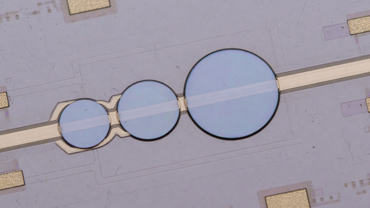
Researchers at Friedrich‑Alexander‑Universität Erlangen‑Nürnberg have shown that re‑orienting a 4H‑SiC wafer from the usual c‑plane to the a‑plane allows silicon‑vacancy (VSi) qubits to be accessed more directly. By fabricating a lateral pin‑diode structure on the a‑plane substrate, the dipole moment of the VSi defect aligns parallel to the wafer surface, enabling out‑of‑plane resonant optical excitation and precise electrical Stark tuning.
Lateral Pin‑Diode on an A‑Plane Substrate
- Device performance – The pin‑diodes block voltages up to –150 V and exhibit reverse leakage currents below 10 pA, reducing charge noise during optical measurements.
- CMOS compatibility – The process uses standard silicon‑carbide CMOS steps, suggesting a path toward large‑scale integration of quantum components.
- Simulation validation – 2‑D Sentaurus TCAD simulations of doping profiles and electric‑field distributions match the experimental data, confirming the design’s feasibility.
Optical and Electrical Characterization of VSi Qubits
- Narrow linewidths – Cryogenic photoluminescence at 4 K reveals optical linewidths of 69.4 MHz (A1 transition) and 75.6 MHz (A2 transition), indicating high‑quality emitters.
- Stark tuning – Applying a reverse bias creates a controllable electric field parallel to the crystal c‑axis, shifting the VSi emission frequency with near‑linear dependence on voltage. This capability is essential for bringing disparate emitters into spectral resonance.
- Quantum sensing potential – Embedding VSi centers within the diode enables in‑situ electric‑field sensing, offering a route to monitor and calibrate power‑electronics devices at the nanoscale.
Implications for Scalable Quantum Technologies
The a‑plane orientation removes the need for complex out‑of‑plane excitation schemes required on c‑plane wafers. Combined with low‑noise diode operation, this architecture supports:
- Scalable quantum photonic integrated circuits (QPICs) – Direct coupling to TE‑polarized planar waveguides becomes straightforward.
- Multi‑qubit entanglement – Precise Stark tuning paves the way for generating indistinguishable photons from multiple VSi centers, a prerequisite for on‑chip entanglement.
- Integrated quantum sensors – The same device can act as a quantum sensor embedded in power‑electronics, providing three‑dimensional electric‑field maps.
Overall, the work demonstrates a practical, CMOS‑compatible route to control and read out silicon‑vacancy qubits, moving solid‑state quantum hardware closer to industrial scalability.
--- For detailed experimental methods and simulation parameters, see the authors’ arXiv preprint.
Hype check
PartlyThe paper presents a new a‑plane device architecture with experimental data, but it is only a preprint and lacks independent verification.
- Peer-reviewed paper, or press release only?Press release only — Only an arXiv preprint is cited
- Error-corrected (logical) qubits, or physical qubits only?Logical / not a qubit claim — No qubit‑count claim; focus is on control of individual VSi qubits
- A new milestone, or a rebrand / restatement?New — First demonstration of a‑plane lateral pin‑diode for VSi control
- Independent confirmation?Not yet — No external replication or third‑party confirmation mentioned
- Does the headline claim match what the source shows?Matches — Headline accurately reflects the reported simplification of VSi control
An editorial assessment of the claim as reported, not a judgment of the company or researchers. Checked against: arxiv.org. How we rate hype →
Source
Read original sourceWhy we picked this
Accepted from curated QuantumUnzipped source (relevance scoring disabled).