A breakthrough in magnetism could make AI chips use dramatically less energy
Brown researchers eliminated the dead‑layer effect in ultrathin multiferroic films, preserving and enhancing their magnetic properties.
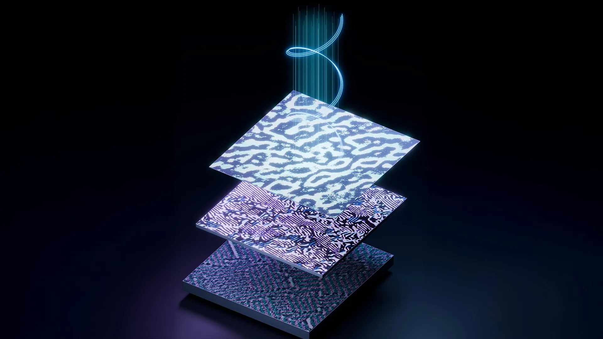
A New Materials Trick Could Slash Future AI Chip Power
Researchers at Brown University have shown that a three‑layer growth method can keep bismuth ferrite—an important multiferroic—ferroelectric and magnetic down to just a few angstroms. The approach removes the long‑standing “dead layer” that normally destroys these properties when the material is made ultra‑thin, and it even induces a novel altermagnetic state that combines the speed of antiferromagnets with the read‑out strength of ferromagnets.
Overcoming the Dead‑Layer Barrier
Multiferroics are attractive for low‑power electronics because a tiny voltage can flip both their electric polarization and magnetic orientation, enabling memory and logic operations with minimal energy. However, when the films are thinned to the dimensions required for modern chips, structural distortions and internal electric fields suppress both ferroelectricity and magnetism—a problem known as the dead‑layer effect.
Brown’s team solved this by depositing bismuth ferrite on a dysprosium scandate substrate that compresses the film, preserving its crystal lattice. A second metallic layer screens the disruptive electric fields. The combined strain and field‑screening keep the material’s multiferroic behavior intact even at near‑atomic thicknesses.
Emergent Altermagnetism
Beyond preservation, the engineered stack gave rise to altermagnetism, a hybrid magnetic order that offers strong, easily detectable signals like ferromagnets while retaining the fast dynamics and lack of stray fields typical of antiferromagnets. This could allow densely packed, high‑speed magnetic components that are still readable with low‑energy circuitry.
Implications for Energy‑Efficient AI Hardware
AI workloads are driving exponential growth in data‑center power consumption. If multiferroic‑based memory or logic can be integrated into CMOS processes, the voltage‑controlled switching could reduce the energy per operation dramatically. The authors caution that the technology is still at the materials‑proof‑of‑concept stage; further engineering will be needed to translate the thin‑film performance into commercial chips.
Looking Ahead
The work, published in Nature Materials, demonstrates a clear path to overcoming a key materials bottleneck. Future research will need to address scalability, integration with existing fabrication lines, and real‑world benchmarking of energy savings in AI accelerators. Nonetheless, the discovery marks a significant step toward ultra‑low‑power computing architectures.
--- Funding was provided by the U.S. Army Research Office, NSF, and the Department of Energy.
Hype check
PartlyThe paper demonstrates a materials breakthrough, but the claim that it will dramatically cut AI chip energy is not yet quantified or independently verified.
- Peer-reviewed paper, or press release only?Paper — Published in Nature Materials
- Error-corrected (logical) qubits, or physical qubits only?Logical / not a qubit claim — Not a qubit‑count claim
- A new milestone, or a rebrand / restatement?New — Eliminates dead layer in ultrathin multiferroics
- Independent confirmation?Not yet — No external replication mentioned
- Does the headline claim match what the source shows?Matches — Headline reflects the reported materials breakthrough
An editorial assessment of the claim as reported, not a judgment of the company or researchers. How we rate hype →
Source
Read original sourceWhy we picked this
Accepted from curated QuantumUnzipped source (relevance scoring disabled).