A tiny defect in a crystal reveals a big quantum surprise
A new computational framework reveals that internal conversion, an overlooked energy‑loss pathway, dominates the excited‑state dynamics of silicon‑carbide spin defects, reshaping predictions for quantum technologies.
Introduction
A recent study from the University of Chicago’s Pritzker School of Molecular Engineering has uncovered a hidden energy‑loss mechanism in silicon‑carbide (SiC) spin defects. By extending first‑principles simulations to capture the full optical cycle—including the notoriously difficult internal conversion process—the researchers explain long‑standing discrepancies between theory and experiment and open new avenues for quantum computing, sensing, and energy‑conversion research.
Why Spin Defects Matter
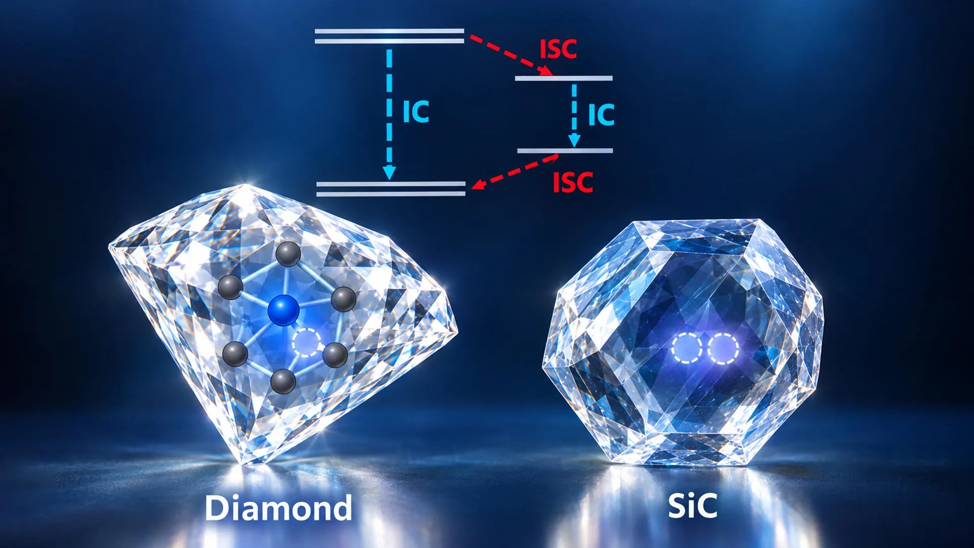
Spin defects—tiny imperfections such as nitrogen‑vacancy centers in diamond or divacancies in SiC—can host stable electron spins that serve as qubits. Their appeal lies in optical addressability: a laser can excite the defect, and the resulting fluorescence or spin state can be read out. To engineer reliable quantum devices, scientists must understand how these defects relax back to their ground state after excitation. Traditionally, two pathways dominate the discussion:
- Radiative decay, where the defect emits a photon.
- Spin‑flip transitions, which change the spin orientation without photon emission.
A third route, internal conversion, transfers electronic energy into lattice vibrations (phonons). This non‑radiative channel has been difficult to model because it requires simultaneous treatment of electronic excitations and thousands of atomic motions.
The New Computational Framework
The Galli group combined several advanced techniques to overcome this hurdle:
- Many‑body wavefunctions describe excited electronic states with high accuracy.
- Exact derivations link each excited state to the vibrational configurations of hundreds of surrounding atoms, eliminating the need to enumerate every configuration individually.
- Implementation in WEST, an open‑source GPU‑accelerated code, enables large‑scale simulations that were previously impractical.
The result is a unified method that predicts both radiative and non‑radiative decay rates across the entire optical cycle.
Surprising Findings in Silicon‑Carbide
Applying the framework to a well‑studied nitrogen‑vacancy center in diamond reproduced known spectroscopy results, confirming the method’s reliability. The real surprise emerged when the team examined a divacancy defect in SiC:
- Internal conversion dominates the triplet‑state lifetime, far exceeding prior estimates.
- This heightened non‑radiative loss reconciles earlier mismatches between calculated lifetimes and experimental measurements.
- The insight suggests that SiC qubits may require engineering strategies—such as strain tuning or isotopic purification—to suppress phonon coupling and extend coherence times.
Broader Implications
Beyond quantum information, internal conversion influences energy‑transfer processes in photovoltaic and photocatalytic materials. By providing a tractable way to quantify phonon‑mediated losses, the new framework can guide the design of more efficient light‑harvesting systems. The authors also note ongoing work to integrate machine‑learning models that could further reduce computational cost, making the approach accessible to a wider community.
Practical Takeaways
- For quantum engineers: Incorporate internal conversion rates when modeling SiC‑based qubits to avoid overestimating performance.
- For materials scientists: Use the WEST‑based workflow to assess non‑radiative losses in any optically active defect or impurity.
- For computational researchers: The study demonstrates the power of combining many‑body electronic structure with GPU‑accelerated algorithms, a template for tackling other complex solid‑state phenomena.
Closing Thoughts
By finally quantifying a hidden decay channel, this work fills a critical gap in our understanding of spin‑defect optics. The ability to predict the full optical cycle paves the way for more accurate material design, whether the goal is a robust quantum processor, an ultra‑sensitive sensor, or a next‑generation solar cell.
Source
Read original sourceWhy we picked this
Accepted from curated QuantumUnzipped source (relevance scoring disabled).