Anderon Releases First Superconducting Quantum PDK
Anderon’s new superconducting quantum PDK offers standardized design blocks and a reference coherence design for 300 mm wafer fabrication, aiming to streamline quantum device development.
Introduction
Anderon, the quantum‑foundry arm of IBM, announced the release of its first Superconducting Quantum Process Design Kit (PDK). Targeted at developers of quantum devices and circuits, the kit bundles a set of design components—qubits, I/O routing elements, amplifiers, and filters—along with a reference design for baseline coherence validation. By delivering these building blocks for Anderon’s 300 mm wafer platform, the company hopes to reduce the time and effort required to move from a laboratory prototype to a manufacturable quantum chip.
What the PDK Provides
The Anderon PDK is organized around three core categories:
- Qubit primitives – Standardized layouts and parameter sets for superconducting qubits that are compatible with Anderon’s wafer‑scale process. These include design rules for Josephson junctions, capacitor geometries, and recommended materials.
- Signal‑routing and I/O components – A library of microwave transmission lines, couplers, and interconnects that facilitate low‑loss routing of control and read‑out signals across the chip. The kit also supplies design guidelines for impedance matching and crosstalk mitigation.
- Amplifiers and filters – Pre‑characterized parametric amplifiers, band‑pass filters, and isolation structures that support high‑fidelity quantum control and measurement. Each element comes with simulated S‑parameters and noise figures to aid system‑level simulation.
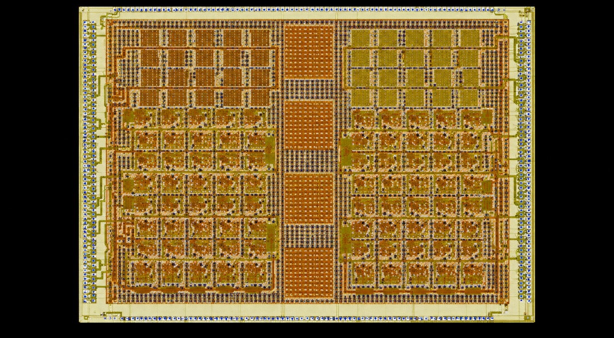
In addition to these libraries, the PDK includes a reference design that demonstrates a minimal quantum processor layout capable of baseline coherence validation. The reference provides electromagnetic simulation parameters, such as participation ratios and loss tangent estimates, enabling designers to benchmark their own layouts against a known target.
Why a PDK Matters for Superconducting Quantum Development
Designing superconducting quantum circuits has traditionally been a highly bespoke activity. Researchers often craft custom mask sets and rely on ad‑hoc simulation models, which can lead to long iteration cycles and unpredictable yields when moving to a commercial fab. A PDK addresses these challenges by:
- Standardizing design rules: Consistent geometry constraints and material specifications reduce the risk of design‑for‑manufacturing errors.
- Accelerating simulation: Pre‑extracted electromagnetic parameters let engineers run accurate system‑level simulations without rebuilding models from scratch.
- Facilitating collaboration: A common component library makes it easier for teams across academia and industry to share designs and compare performance metrics.
- Bridging innovation and scale: By providing a manufacturable pathway early in the design process, the PDK helps innovators transition from proof‑of‑concept chips to larger‑scale production runs.
Early‑Access Licensing and Next Steps
Anderon is offering early access to the first‑generation PDK through a license agreement. Interested parties can contact the Anderon team to obtain the kit, evaluate its components, and provide feedback that will shape future revisions. The early‑access model serves two purposes: it allows developers to begin integrating the PDK into their design flows, and it gives Anderon real‑world usage data to refine the library and expand its coverage.
Practical Takeaways
- Start with the reference design: Use the provided baseline layout to validate your simulation tools and get a feel for the expected coherence metrics on Anderon’s 300 mm process.
- Leverage the component libraries: Incorporate the pre‑characterized qubit, routing, and amplifier blocks to reduce custom mask work and focus on higher‑level architecture.
- Plan for licensing: Engage with Anderon early to secure access, especially if your roadmap includes fabrication on their wafer platform.
- Monitor updates: As the PDK evolves, new components and refined parameters will be added, so maintain a feedback loop with the Anderon team.
Conclusion
Anderon’s superconducting quantum PDK marks a significant step toward a more mature quantum‑hardware ecosystem. By packaging essential design elements and a reference coherence testbed for its 300 mm wafer process, the kit promises to streamline the path from circuit conception to silicon‑based quantum fabrication. Early adopters who integrate the PDK into their workflows can expect faster design cycles, more predictable manufacturing outcomes, and a clearer route to scaling their quantum technologies.
Source
Read original sourceWhy we picked this
Accepted from curated QuantumUnzipped source (relevance scoring disabled).