How electrons find their way to diamond's quantum defects
A new study shows electrons tunnel from nitrogen atoms to NV centers in diamond, explaining how these quantum defects regain charge.
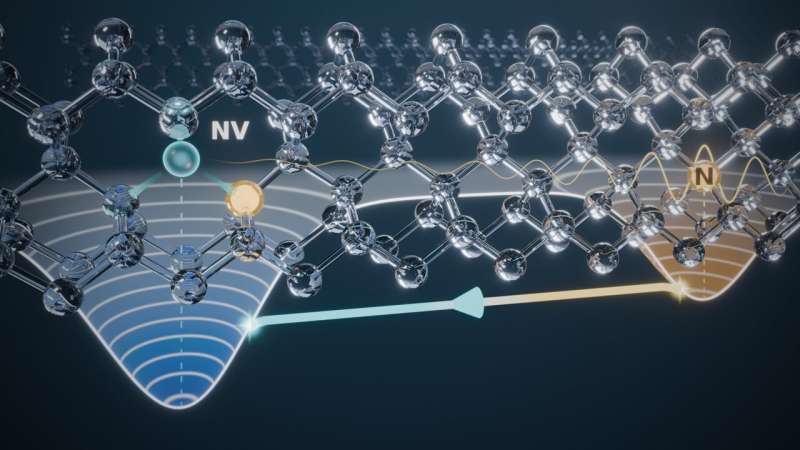
How Electrons Find Their Way to Diamond’s Quantum Defects
Diamond’s nitrogen‑vacancy (NV) centers are prized for quantum computing, networking, and ultra‑sensitive sensing because they can act as room‑temperature qubits. Their operation hinges on holding an extra electron; when that electron is lost, the defect becomes inactive. Researchers from Germany, Lithuania, and the United States have now identified the microscopic mechanism that restores the missing electron.
Quantum tunneling replaces thermal activation
In most semiconductors, heat can free electrons from donor defects, allowing them to wander and be captured elsewhere. Nitrogen atoms in diamond bind electrons far too tightly for thermal release, leaving the NV center stranded. The new work, published in Physical Review Letters, demonstrates that the electron does not need to climb over the energy barrier—it tunnels directly through it. This quantum‑mechanical shortcut is accompanied by a burst of energy that the nitrogen atom efficiently absorbs via vibrational motion of the crystal lattice.
Experimental proof across many time scales
To capture the slow recovery of NV centers, the team used a novel pump‑probe scheme. A pulsed red laser removes the electron (pump), while a continuous weak laser monitors the NV’s optical absorption (probe). By extending the observation window from nanoseconds to seconds, they could separate the fast internal relaxation of the NV from the much slower charge‑replenishment process. Diamonds with higher nitrogen concentrations showed rapid recovery, whereas nitrogen‑poor samples exhibited recovery times ranging from nanoseconds to hours, matching the tunneling model’s distance‑dependent predictions.
Implications for quantum technologies
The findings clarify why NV‑based devices sometimes suffer from erratic performance: the stochastic nature of electron tunneling introduces timing jitter that can span many orders of magnitude. Armed with this knowledge, engineers can design diamonds with strategically placed nitrogen donors—or introduce alternative impurity species—to stabilize the charge state and improve device reliability. Moreover, the mechanism likely applies to other tightly‑bound defects in materials such as LED phosphors, radiation detectors, and insulating layers in microelectronics.
Looking ahead
Beyond diamond, the study opens a broader research direction: investigating electron‑tunneling charge transfer in a variety of solid‑state defects where thermal activation is ineffective. By combining quantum‑mechanical simulations with long‑timescale optical measurements, future work can map out optimal defect engineering strategies for a new generation of quantum sensors and processors.
Reference: Audrius Alkauskas et al., “Charge State Equilibration of Nitrogen‑Vacancy Center Ensembles in Diamond: The Role of Electron Tunneling,” Physical Review Letters (2026). DOI: 10.1103/l3yf‑k48t.
Hype check
PartlyThe paper provides a peer‑reviewed theoretical and experimental demonstration of tunneling, but no independent replication is reported.
- Peer-reviewed paper, or press release only?Paper — Published in Physical Review Letters
- Error-corrected (logical) qubits, or physical qubits only?Logical / not a qubit claim — Not a qubit‑count claim
- A new milestone, or a rebrand / restatement?New — First experimental evidence of tunneling‑mediated charge recovery
- Independent confirmation?Not yet — No external confirmation mentioned
- Does the headline claim match what the source shows?Matches — Headline accurately reflects the tunneling mechanism described
An editorial assessment of the claim as reported, not a judgment of the company or researchers. Checked against: phys.org. How we rate hype →
Source
Read original sourceWhy we picked this
Accepted from curated QuantumUnzipped source (relevance scoring disabled).