New atomic cell platform speeds up chip-scale clock design
Researchers have introduced an inkjet‑based method to fabricate MEMS atomic cells with controllable nitrogen pressure, speeding up chip‑scale atomic clock development.
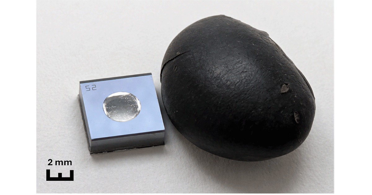
A Faster Path to Better Chip‑Scale Atomic Clocks
A team from Japan’s National Institute of Information and Communications Technology (NICT) and partner labs has unveiled a new manufacturing platform for micro‑electromechanical systems (MEMS) atomic cells. By using ink‑jet deposition of rubidium azide (RbN₃) microparticles, the process lets engineers set the nitrogen‑gas pressure inside each vapor cell at the wafer‑level, rather than discovering it only after the cell is built. This tighter control promises to accelerate the design‑optimisation loop for chip‑scale atomic clocks, which are critical timing sources for navigation, telecommunications and autonomous‑vehicle systems.
---
Ink‑Jet Deposition Gives Precise Gas‑Pressure Control
Traditional MEMS vapor‑cell fabrication relies on bulk‑process steps that leave the internal gas composition largely unknown until after the cell is sealed and tested. The new platform deposits a measured amount of RbN₃ onto each cell using a commercial ink‑jet printer. When heated, the compound thermally decomposes, simultaneously releasing rubidium vapor and nitrogen gas. The amount of deposited material correlates linearly with the resulting nitrogen partial pressure, allowing designers to predict and set the pressure before the wafer is diced.
This capability eliminates a costly trial‑and‑error cycle. Engineers can now fabricate arrays of cells with systematically varied nitrogen pressures, evaluate coherent‑population‑trapping (CPT) resonances across the array, and quickly identify the pressure range that yields the narrowest resonance and best clock stability.
---
Impact on Chip‑Scale Atomic Clock Performance
Chip‑scale atomic clocks (CSACs) rely on the CPT resonance of rubidium atoms confined in a tiny vapor cell. The resonance linewidth and contrast are highly sensitive to the buffer‑gas pressure; too much nitrogen broadens the line, while too little reduces the signal strength. By delivering the desired nitrogen pressure directly during wafer processing, the new platform enables:
- Predictable resonance characteristics – designers can model CPT behavior with confidence, reducing the need for post‑fabrication tuning.
- Higher short‑term stability – optimized pressure yields narrower linewidths, improving frequency stability on the order of 10⁻¹¹ to 10⁻¹² over one second.
- Scalable production – the ink‑jet step integrates with existing MEMS wafer‑fab lines, supporting high‑volume manufacturing without major equipment changes.
These improvements are especially valuable for applications that demand precise timing in harsh or remote environments, such as satellite navigation, deep‑space probes, and autonomous‑vehicle fleets.
---
Looking Ahead: From Prototype to Production
The researchers emphasize that the platform is compatible with standard wafer‑level processes, meaning that commercial foundries could adopt the technique without extensive retooling. Future work will focus on:
- Fine‑tuning cell geometry – exploring different cavity shapes and coatings to further enhance CPT contrast.
- Integrating with packaging – ensuring that the pressure‑control benefits survive the final hermetic sealing steps.
- Extending to other atomic species – testing whether the method works for cesium‑based cells, which are used in some timing standards.
If these steps succeed, the time from concept to a production‑ready CSAC could shrink dramatically, helping the broader timing‑infrastructure ecosystem keep pace with the growing demand for ultra‑precise, low‑power clocks.
---
Practical Takeaway
The ink‑jet‑based atomic‑cell platform represents a concrete engineering advance that removes a major bottleneck in CSAC development. By giving designers direct, wafer‑level control over nitrogen pressure, the method speeds up the optimisation cycle, improves clock performance, and fits within existing manufacturing flows. Stakeholders in navigation, telecommunications and autonomous‑system markets should watch for commercial roll‑outs of this technology in the next few years.
Hype check
Not a research claimThe story reports a new fabrication method for MEMS atomic cells; there is no performance claim to overstate, just a research announcement.
We rate research and technical results only. How we rate hype →
Source
Read original sourceWhy we picked this
Accepted from curated QuantumUnzipped source (relevance scoring disabled).