NVision Demonstrates Addressable Molecular Spin-Photon Interface and Partners with HyperLight for Integrated Photonic Hardware
NVision has shown single‑molecule spin‑photon control and teamed with HyperLight to integrate molecular qubit films onto thin‑film lithium‑niobate photonic chips, aiming for scalable quantum photonic hardware.
Introduction
NVision Quantum Technologies announced a breakthrough in quantum hardware: an addressable organic molecular spin‑photon interface that can be deposited directly onto thin‑film lithium‑niobate (TFLN) photonic integrated circuits (PICs). The result, demonstrated in a peer‑reviewed study, shows coherent control, optical initialization, and readout of individual synthetic carbene molecules, and marks the start of a development partnership with HyperLight Corporation to bring this capability to commercial photonic platforms.
Molecular Spin Architecture and Performance
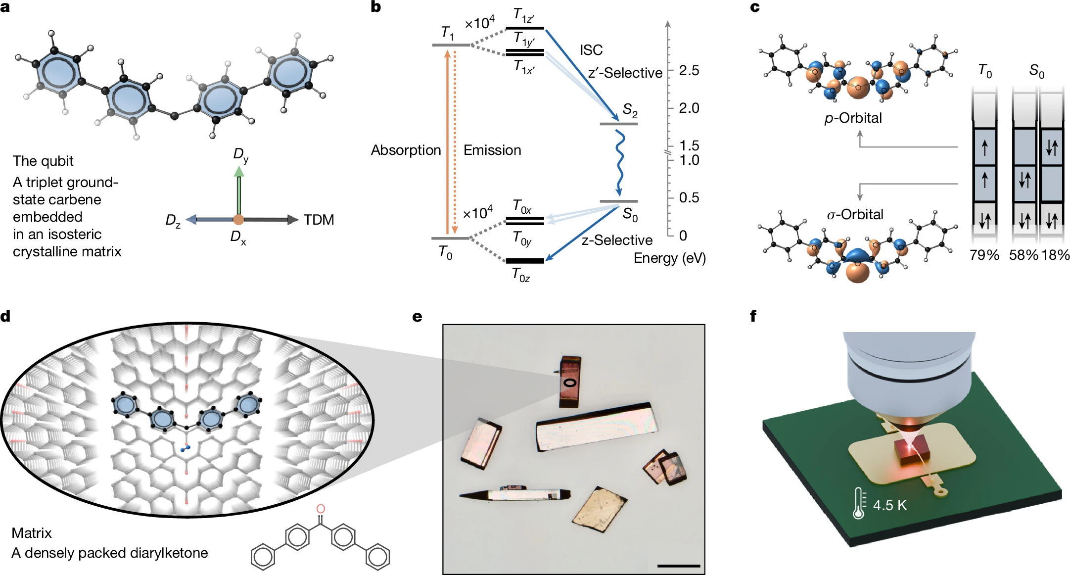
The core of the platform is a specially engineered carbene molecule—an aromatic biphenyl‑substituted divalent carbon—embedded substitutionally in an isosteric organic host crystal. A focused laser triggers a photo‑elimination reaction that creates a stationary qubit with sub‑micrometer placement precision. Operating at 4.5 K, the electron spin benefits from a large zero‑field splitting (|D| = 11.16 GHz, |E| = 0.54 GHz), which suppresses magnetic noise from surrounding hydrogen nuclei.
Key experimental metrics include:
- Zero‑phonon line (ZPL) emission at 595.04 nm for optical addressing.
- Optical linewidth of 38 ± 2 MHz, providing spectrally sharp transitions.
- Single‑photon purity g²(0) = 0.142, confirming isolated single‑molecule emission.
- Spin coherence T₂ (XY8) = 2.2 ± 0.3 ms, achieved with dynamical decoupling.
- Spin‑lattice relaxation T₁ = 21 ± 2 ms, setting the upper bound for spin lifetime.
These figures demonstrate that a single organic molecule can act as a reliable quantum emitter with millisecond‑scale coherence, comparable to many solid‑state color‑center systems while being compatible with solution‑based processing.
Integration with Photonic Integrated Quantum Circuits
Through the partnership with HyperLight, NVision plans to deposit carbene thin films directly onto HyperLight’s TFLN chiplet platform. The TFLN waveguides will route photons emitted by the molecular spins, enabling optical interconnects between qubits without the dense wiring required in conventional semiconductor chips. In NVision’s broader Photonic Integrated Quantum Circuits (PIQC) architecture, the molecular electron spin serves as the optical interface, while nearby nuclear spins (e.g., site‑selected ^13C isotopes) act as long‑lived memory registers.
The design tolerates up to 70 % optical loss and separates spin transition frequencies by at least 1.555 GHz to reduce cross‑talk. However, scaling to wafer‑level production will require uniform molecular film deposition, low‑loss coupling between molecules and waveguides, and high‑fidelity entangling gates across distinct qubits. NVision targets a prototype on‑chip demonstration by the end of 2026 and a roadmap toward fault‑tolerant logical systems by 2030.
Outlook and Practical Implications
The molecular spin‑photon interface offers several practical advantages:
- Manufacturing Compatibility – Solution‑processed molecules can be deposited using standard thin‑film techniques, potentially lowering fabrication costs compared with cleanroom‑only color‑center creation.
- Modular Integration – Direct coating onto TFLN chiplets enables a plug‑and‑play approach for quantum photonic modules, facilitating rapid iteration and heterogeneous integration with existing silicon photonics.
- Scalable Coherence – Millisecond‑scale T₂ times at 4.5 K suggest that modest cryogenic infrastructure (helium cryostats) can support sizable qubit arrays without the complexity of dilution refrigeration.
Realizing these benefits will hinge on overcoming deposition uniformity and coupling efficiency challenges, as well as demonstrating multi‑qubit entanglement on the integrated platform. If successful, NVision’s approach could complement semiconductor‑based color centers and trapped‑ion systems, expanding the toolbox for building large‑scale quantum processors and quantum networks.
--- This article synthesizes the information provided in the NVision announcement and related technical brief, focusing on the scientific results and their implications for quantum hardware development.
Source
Read original sourceWhy we picked this
Accepted from curated QuantumUnzipped source (relevance scoring disabled).